

The quality of printed circuit boards (PCBs) directly affects the reliability, and safety of electronic devices. By conducting the right quality checks at the right stages, electronics manufacturing service (EMS) providers can detect defects early, ensuring compliance with original equipment manufacturers’ (OEM) requirements. This not only reduces production costs and enhances product quality but also safeguards devices from safety hazards and prevents costly failures, all of which contribute positively to the OEM’s reputation.
This article explores the key inspection and testing methods that help maintain high standards in PCB assembly.
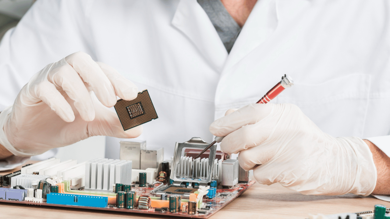
Visual and Optical Inspection Methods
Manual inspection is one of the most basic budget ways to assess PCB assemblies at various production stages, including the application of solder paste, component placement, and curing of solder joints. The reliance on the manual assessment techniques it involves, however, makes this method more subjective than those relying on more advanced equipment.
For example, industry experts like Poland-based Assel prioritise automated techniques like inline automated optical inspection (AOI) to detect early assembly flaws such as missing components or misalignment.
In addition, they employ 3D automated solder paste inspection (SPI) to ensure precise solder paste application, preventing defects caused by insufficient or uneven paste distribution. Automated methods help companies reduce manual errors, improve consistency, and accelerate the detection of potential issues.
Internal and Hidden Defect Detection
While automated visual testing methods can be highly effective, they are limited to surface inspection. To detect internal or hidden issues, EMS providers should implement other techniques, for instance, 3D automated X-ray inspection (AXI).
AXI allows companies to perform a detailed scan of each layer of the PCB, which helps to identify defects like improper solder paste distribution or hidden issues beneath components like ball grid arrays (BGAs). This method ensures that even internal flaws, invisible to visual inspection, are detected early in the process.
However, AXI can be expensive and is usually reserved for high-priority or complex assemblies where surface inspections alone may not be enough.
Functional Testing
While helpful in quality control, the methods mentioned above are not meant to assess the functionality of PCBs. For this purpose, EMS providers should employ dedicated functional testing (FCT), which is a critical step in ensuring that completed products function as intended. These tests are time-consuming but crucial for verifying that all components work together seamlessly and meet the product’s specifications, which indicates their reliability in real-world scenarios.
Typically conducted after in-circuit tests (ICT), which quickly identify assembly errors such as incorrect components or short circuits, FCT ensures that any issues not detected earlier are addressed before the product reaches the market.
Safety and Stress Testing
To assess the durability and reliability of PCBs under various conditions, particularly regarding electrical safety, contract manufacturers conduct safety and stress testing. These tests help identify faulty products before release, ensuring that they meet stringent safety standards.
Safety and stress testing includes the burn-in test, which exposes the product to high temperatures over an extended period to detect early failures or weaknesses. However, it is important to avoid excessive wear on components during testing, as this could shorten the product’s lifespan.
Another key method is Hi-Pot PCB Testing, where the PCB is subjected to high voltage to check its ability to withstand voltage spikes without damage. This test is particularly important for high-voltage applications, as it ensures that the insulation and dielectric materials are adequate to prevent dangerous electrical failures.
Environmental Testing
While safety and stress testing may overlap with environmental testing to some extent, the latter specifically focuses on simulating the various environmental conditions a PCB may face throughout its operational lifespan, including the periods of operation, transportation, and storage.
These simulated extreme environments include significant temperature fluctuations, high humidity, and exposure to mechanical stress. Environmental tests for PCB assessment often involve climate testing techniques that examine the device’s resistance to temperature extremes, humidity, corrosion, UV exposure, and ingress.
Conclusions
Ensuring the quality, safety, and reliability of PCBs is impossible without thorough inspection and testing methods. From automated optical inspections to functional and environmental testing, each method plays a crucial role in detecting potential issues early and maintaining high standards.
By implementing these rigorous processes, EMS providers can reduce costs, improve product quality, and protect both the devices and the manufacturer’s reputation. To partner with a reliable EMS provider that prioritises comprehensive quality inspection, visit asselems.com.